Tuesday, August 17, 2010

Circuit Two (Power Circuit)

Circuit 2 (Using Linea Regulator)

Adjustable linear regulator is used to support the input voltage and output voltage. In this circuit the supply voltage is 12V and various components are used to far the purpose of voltage drop and an LED to physically see if the circuit is working, (warning light) and capacitors are used to store energy and release back when switch is off.
The purpose of this circuit is to find out the value of voltage out  as we did in our calculation which was 5V this gain value depends on the value of resistors R3 and R2 from the formula.


V Out = V Ref ( 1 + R3 / R2 )                                              Ld = 20mA = 0.02 A
5V = 1.25 ( 1 + R3 / R2 )                                                     V = 5V - 1.8V
4 - = R3 / R2                                                                        Ld = 3.2V
3 R2 = R3                                                                            R1 = 3.2V / 0.02A = 160 Ohms

Zd = 22V
D1 = 0.7V
D2 = 0.7V
R1 = 160 Ohms
R2 = 220 Ohms
R3 = 660 Ohms


Test

Checked the available voltage in various points, the result was positive checked the circuit for the voltage drop in D13 which is 0.75V and the voltage drop is 10.70V for both D15 Zener diode and C15 (capacitor), voltage drop across D12 as 5.02V, across R2 is 1.24V, across R3 is 3.78V, across C16 is 5V, across R1 is 3.02V and across LED is 2.00V.
From our test it showed that output voltage is exactly 5.02V that is what we got in our calculation.


The output voltage in the figure below is show 5.16V as the input was 13V


Problems

When i built the circuit from the diagram which was designed on the Loch Master software, the results were negative, first i have put the NO 13 input diodes in opposite side which was blocking the voltage supply to the circuit, and after finding the problem I have overcome the problem by positioning the diodes correctly. The output reading was also showing 12V which was suppose to show 5V. The cause for that was poor connection and i have fixed the problem by soldering correctly and tested the circuit afterwards, it worked correctly. The readings of my circuit were exactly as stated under tests above.


Reflection

I have came across few issues while building this circuit, however after digging a bit deeper into the problem i have found the root cause for them and overcame all problems, this was a good lesson and it has made the process much easier for my next circuit.


Sunday, August 15, 2010

Experiment No. 8


I have created the following circuit which is 470R for RC and BC457 NPN Transistor.


I have picked five resistors between 2K2 and 1M for Rb. I have have placed these resistors to see when Vce is saturated switch region and when it is in the active amplifier region. I have also used other different types of resistors to measure and record voltage drop across Vce and Vbe. Also measure and record the current for Ic and Ib, then i have changed the Rb resistor and did all the measurement and recorded the new reading. The output of my measurements are illustrated in the following table:


Rb
2.2K W
Vbe
0.78V
Vce
0.04V
Ib
1.91mA
Ic
6.09mA
Rb
55K W
Vbe
0.73V
Vce
0.10V
Ib
0.1mA
Ic
0.61mA
Rb
220K W
Vbe
0.60V
Vce
3.27V
Ib
2.3mA
Ic
7.7mA
Rb
270K W
Vbe
0.70V
Vce
1.13V
Ib
0.05mA
Ic
4.7mA
Rb
1M W
Vbe
0.67V
Vce
2.85
Ib
0.11mA
Ic
1.1mA


During this experiment voltage dropped between collector and emitter, the bigger the resistor the high voltage drop reading between Vce and the smaller the resistor was the less voltage drop was between C and E.

During this experiment for Vbe there was a slightly voltage drop in Vbe but not a major change.

In my experiment in Ib the current flow was dropping and in increasing.

Resistance Rb: It resistricts the current flow along Ib, so bigger the resistance the less the current flow to the base.

During Ic experiment it was the same as above as we placed a bigger resistance in Rb, it resistricted the current flow to the collector.


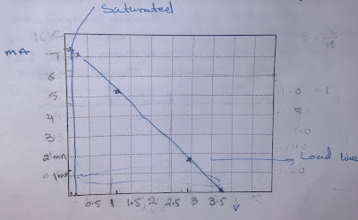
Load line represents Ic again Vce, the higher current flow to Ic, the lower voltage drop (Vce) or wise-versa. Transistor is fully opened in saturated area so it means more current flow in active area, the transistor is active in active area (Increase and Decrease) the flow of the current depends on the resistance (Rb) in cut off area more voltage drop, more heat generated and less current flow, further voltage drop and more heat generated would damage the transistor. for instance, increase the current flow from base to emitter will increase the current flow from collector to emitter

Friday, August 13, 2010

Circuit One (Injector Circuit)

Circuit One (Bipolar Junction Transistor Circuit)

From the data sheet:

20 mA : LED
1.8V : LED (Voltage Drop)
NPN :  547 Transistor
Ic :  100mA
Ib :  5mA
Vce : 0.2V
Vbb = 5V
Beta = 100


Calculation

Saturation
Rb = Vce - Vd be / Ib
= 5V - 0.9V / 0.005 = 4.1 / 0.005 = 820 Ohms

Active Current Gain
Ib = Ic / B
= 0.02 / 100 = 0.0002A
Rc = Vcc - VD - VD LED / Ic
= 12V - 0.2 - 1.8 = 10 / 0.02 = 500 Ohms
Rb = Vbb - VD / Ib
= 5 - 0.9 / 0.2 = 20.5 K Ohms
The Voltage Drop Reading around the Circuit is Shown in the Figure Above

The circuit illustrated above is a Bipolar Junction Transistor circuit which is consisted of two LEDs in parallel, 4 resistors and 2 transistors which we will be focusing on its function. BJT has 3 terminal electronic devices constructed of dope semiconductor materials which is used in switching application, this BJT circuit needs only 5V to switch and a 20mA lamp which means that 5V will go through base to emitter to open the gates for Vce which is a higher voltage to cause the signal or the LED to flash and this process takes place in active region of transistor, Normally transistors has 3 regions.
  1. Active Region: where power dissipation is very high.
  2. Saturation Region: with both junctions forward base BJT saturation mode facilitates high current conduction from emitter to the collector which is a closed switch.
  3. Cut off Region: this is the opposite to saturation, both junctions are reverse base, there is very little current flow which corresponds to an open switch.
The easy and more efficient way to find three regions and calculate the current gain is the graph of Vce vs Ic for different levels of Ib and the common Emitter circuit B which is the ratio between collector current and base and representing Beta = Ic / Ib

The two pulsing terminals which are only 5 volts going through base to Emitter (Vbe) and this will opens the gates for the collector to emitter (Vce) the path way for the current to flow and cause the LED to flash, this flash of LED depends on the frequency of pulses from the oscilloscope, the higher the frequency of pulses the faster the LED flashes.


Test
Supplying 12V to the circuit with two pulsing terminals connected to 5V to open the gates for Vce.
Checked the available voltage as illustrated in the figure below:


Problems
The only problem which i have came across while making this circuit was that i have placed the resistors on the board on straight line which were connected to Vs.
After finding the problem i have resolved the issue.


Reflection
Making the circuit was not a difficult task, however i have still made few minor mistakes which i have learned from those mistakes and i am confident that i would be able to make a much better circuit in future.

Wednesday, August 4, 2010

Experiment No. 7

Transistor as Switch

Components: 1 x Small Signal NPN transistor, 2 resistors.
Exercise: Connect the circuit as shown below and switch on the power supply.


Connect the multimeter between base and emitter ( 0.80V )
Note the voltage reading and explain what this reading is indicating.

In this switching circuit which simply states that the sum of voltages around a loop or closed path is equal to zero.

VCC = IC RC + VCE

VCC - IC RC - VCE = 0      
15 - 14.2 - 0.8V = 0


Connect the multimeter between collector and emitter ( 0.05V )
Note the voltage reading and explain what this reading is indicating.


In the plot given below what are the regions indcated by the arrows A & B?
A Region: The current flow which is saturated or fully open
B Region: The voltage drop or cut off region.


How does a transistor work n these regions? Explain in details.
The voltage drop is directly related to current flow IC, if there is a high voltage drop there will be low current flow or rise.


What is the power dissipated by the transistor at Vce of 3 Volts?
B = IC / Ib
14 / 0.5 = 28

PD = IC * Vce
14 * 3 = 42 mw

What is the Beta of this transistor at Vce 2,3 & 4 volts?
Vce 2 B = IC / Ib
20 mA / 0.8 m A = 25 mA

Vce 3 B = IC / Ib
14 mA / 0.5  mA = 28 mA

Vce 4 B = IC / Ib
5 mA / 0.2 mA = 25 mA

Experiment No. 6

Bipolar Junction Transistors (BJT)
BJT are made of three layer which are semiconductor "sandwich" which are either PNP or NPN. In BJT two diodes are connected back to back which can be tested with a multimeter's "Diode Check" function shown in the figure below. 


I have a multimeter which has Diode test function for checking the PN junctions which will display the actual forward voltage of PN junction and not just whether or not it conducts current.
If both PN junctions facing other way in NPN transistors then the meter reading would be exactly opposite.
Low voltage reading with the red (+) on the base is the opposite condition for the NPN transistor. If the multimeter with diode function is used in this test it will be found that the emiter-base junction possesses a slightly Higher forward voltage drop than the collector base junction. 


Transistor symbol and semi conductor construction


Identify the legs of your transistors with a multimeter. For identifying and testing purposes refer to the representation shown above.


Diode test (V) meter readings
Transistor Number
VBE
VEB
VBC
VCB
VCE
VEC
NPN
C557
.894
OL
.885
.885
OL
OL
PNP
C547
.886
.885
.883
.894
OL
OL


Experiment No. 5 Capacitor

The Capacitor


Function of Capacitor:


Capacitors store electric charge. They are used with resistor and timing circuits because it takes time for a capacitor to fill with charge. They are used to smooth varying DC supplies by acting as a reservoir of charge. They are also used in filter circuits, because capacitors easily pass AC charging signal and block DC constant signal.


Capacitance

This is a measure of capacitors ability to store charge. A large capacitance mean that more charge can be stored. Capacitance is measured in farads symbol (F). However 1F is very large, so pre fixes are used to show the smaller values.
m Means 10 Power –6 (Millionth) so 1000000 m F = 1F
n Means 10 Power -9 ( Thousand Millionth)  1000nF = 1m F
P Means 10 Power -12 (Million-Millionth) 1000PF = 1nF


Identifying Capacitors "Size"

The following table can be used to figure out the capacitance if the Farad "size" is not printed on the capacitor and EIA code might be listed on the capacitor.


mF
nF
pF
EIA Code
0.00001*
0.01
10
100
0.0001*
0.01
10
101
0.001
1.0 (1n0)
1,000
102
0.01
10
10,000*
103
1.0
1000*
100,000*
104
1.0
1000*
1,000,00*
105
10.0
10,000*
10,000,00*
106


RC Time Delay or “Charging Time”

R * C * 5 = T

Capacitor Charging Circuit

Components: 1 x resistor, 1 x capacitor, 1 x pushbutton N/O switch.

Exercise: Calculate how much time would capacitor take to charge up following by connecting the circuit shown in the figure above. Measure time taken by the capacitor reaching the applied voltage on an oscilloscope.


Circuit number
Capacitance (uF)
Resistance (K W)
Calculated Time (ms)
Observed Time (ms)
1
100
1
500ms
470
2
100
0.1
50ms
50
3
100
0.47
230ms
240
4
330
1
1650ms
1600


How does changes in the resistor affect the charging time?


The initial charge is fast, however overtime the charging process is showing down as it charges and it almost gets to zero which means there is no capacitor for further charge.

How does charges in the capacitor affect the charging time?
The larger the capacitor is the longer it will take to charge and there would be less resistance in the circuit which will make the capacitor to charge faster.